MIT-Guided Researchers Stacking MicroLEDs To Pack More Pixels Into Small Displays
March 2, 2023 by Dave Haynes
MicroLED and even miniLED area already pretty much at a level of development maturity that viewers can be inches from a screen and not really see any gaps between pixels, but there is an ongoing push to get the density of pixels even tighter – albeit for small displays versus giant video walls.
Display Daily has an interesting but (warning) quite technical post up on its site about efforts to stack teeny microLED light emitters, which would pack more of them into a defined area for uses like AR and VR headsets, and perhaps wearables.
I should reinforce here that for most digital signage/video wall applications, super-dense pixel counts would be overkill. But the R&D is nonetheless interesting.
A team of 34 researchers from the US and South Korea and headed by Jiho Shin of the Massachusetts Institute of Technology (Cambridge, MA) are developing means to fabricate vertically stacked arrays of microLEDs.
Warning: technical stuff ahead …
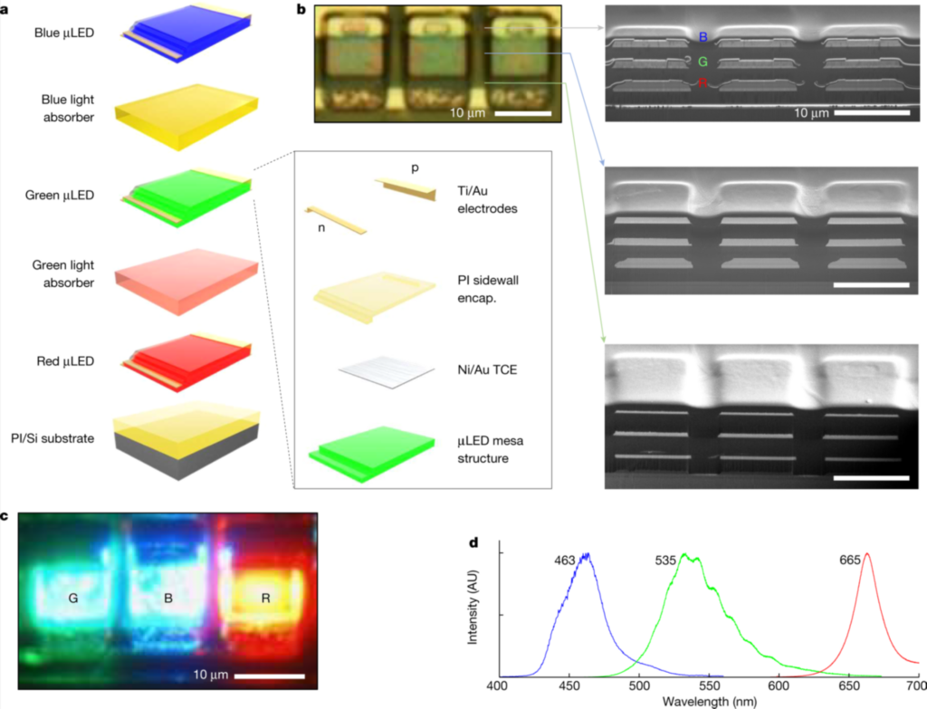
Augmented, virtual and mixed reality headsets require a full color display that has an extremely high pixel density and an extremely small physical size. MicroLEDs have the potential to meet these requirements. Unfortunately, it has been difficult to realize this potential using conventional microLED display fabrication technology. This is due, in part, to the fact that in a conventional array the red, green and blue microLEDs are arranged in a side by side pattern. One means to address this problem is by stacking freestanding red, green and blue LED membranes and fabricating from the top down. Perfecting this technology was the focus of the research undertaken by the team.
Details of the approach investigated by the researchers were reported in a recent article by the team. It is entitled “Vertical full-colour micro-LEDs via 2D materials-based layer transfer.” In this article, the approach developed by the team is described as a “two dimensional materials-based layer transfer technique that allows the growth of red, green and blue LEDs of near submicron thickness on two dimensional material coated substrates via remote or Van der Waals epitaxy, mechanical release and stacking of LEDs followed by top down fabrication.”
More specifically, to produce red AlGaAs-based LEDs, the researchers used graphene, coated on a GaAs wafer. To produce InGaN-based green and blue LEDs, the researchers used hBN on sapphire wafers. (hBN stands for hexagonal boron nitride.) The graphene red LEDs were transferred using remote epitaxy, while the hBN blue and green LEDs were removed using Van der Waals epitaxy. The researchers also demonstrated vertical integration of blue microLEDs with silicon membrane transistors for active matrix operation.
The result of this R&D work is full color, vertically-stacked microLEDs that have a density of 5,100 pixels per inch, with the light emitters just 4 microns in size. For context, anything smaller than 100 microns is considered MicroLED.
You can read the full post here (thought it MAY be paywalled … I pay).
Leave a comment