Daktronics Invests In MicroLED Start-Up X Display
February 29, 2020 by Dave Haynes
Direct view LED manufacturer Daktronics evidently sees microLED as part of its indoor display future, having announced it was part of a Series A investment round in X Display Company (XDC), a Raleigh-Durham, NC start-up that “creates and owns leading intellectual property (IP) and capabilities in microLED mass transfer technology.”
“We see a lot of promise in microLEDs and the products we can produce with this technology,” says Daktronics President and CEO Reece Kurtenbach, whose company is based in Brookings, SD. “We believe XDC is a great partner, with IP and expertise in both the production processes and core technologies needed to produce microLED displays. In conjunction with our participation in this investment round, we are also cooperating on several developments and plan to announce additional product offerings for the Narrow Pixel Pitch (NPP) marketplace later this year.”
“With our roots in mass transfer technology, we’re expanding into the LED space with a significant amount of potential in the large display market,” says XDC CEO Randolph Chan. “We’re excited about this opportunity to develop products with Daktronics, as well as the potential for displays of many different types to leverage our technologies. We look forward to the developments we can bring to life while working together.”
The announcement does not say what kind of money Daktronics put in.
MicroLEDs, says the press release announcing the investment, are less than 50 microns in size and significantly reduce the space need to create pixels that form an image on a display. MicroLEDs are thin, lightweight and power-efficient solid-state devices that emit light that can be manufactured as semiconductor wafers on both flexible and rigid substrates, making them highly suitable for use in full-color displays.
The most pure example of microLED has been the Sony Crystal LED. There are other manufacturers marketing product as microLED that display nerds would say is really miniLED, but there are now rigid standards on how the tech is categorized or marketed. Small and fine are big things in LED, so micro sounds better than mini.
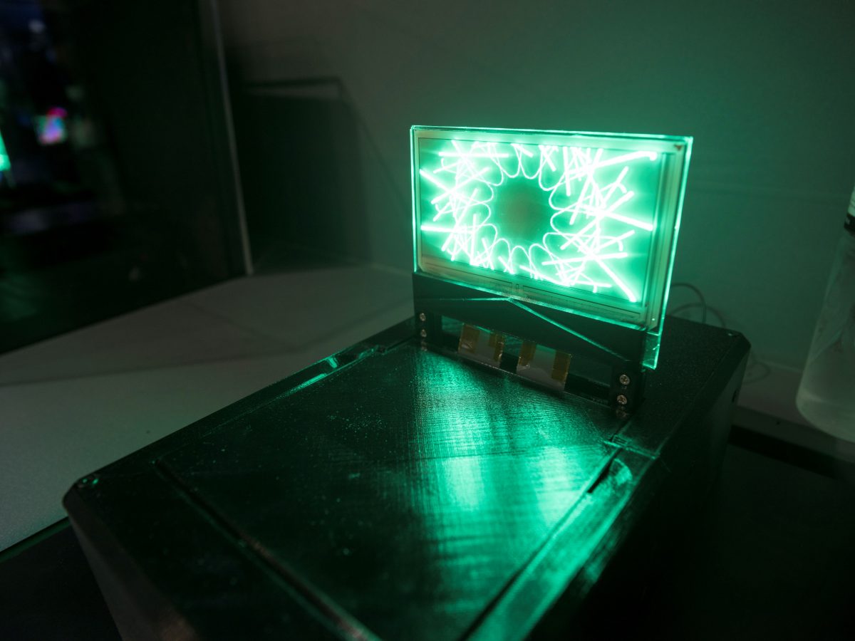
I saw a small X Display prototype last year at Touch Taiwan, in Lextar’s stand. It did not need a conventional backplane or plate, and sat on glass. It could also push 30,000 nits of brightness, which was kind of mind-wobbling.
The tech is, as I wrote from Taipei, intriguing on a whole bunch of levels. The Raleigh, NC company – working with Lextar – says it has individual microscopic level integrated circuits for each LED light, which would remove the need for fabrication plant tech that can cost billions. It also means you could have active, super-high resolution window glass capable of doubling up as displays, with very high transparency.
I don’t normally include company boilerplate in posts, but here’s the background on XDC.
XDC is a leader in the research, development and commercialization of microLED and microIC technologies and semiconductor components for use in display applications. In addition, XDC has developed one of the premier mass transfer process technologies that enable the manufacture of very large displays.
XDC has established a significant portfolio of proprietary microLED technologies, microelectronic components, and digital architecture primarily through XDC’s internal R&D efforts as well as licensed patents from the University of Illinois Urbana-Champaign (UIUC). XDC currently owns, exclusively licenses or has the sole rights to sublicense more than 400 patents (issued and pending) worldwide.
XDC believes that microLEDs offer potential advantages over competing display technologies with respect to brightness, power efficiency, contrast ratio, viewing angle, video response time, form factor and manufacturing costs. XDC’s technology leadership and intellectual property position enables them to capture a significant share of the overall display market as their technology is broadly adopted.
I don’t have the engineering education or intelligence to explain this all that well, but in the lowest common denominator terms I operate well in, the attraction here for Dak and other companies is the process to “mass transfer” the LED die during manufacturing. Conventional direct view LED manufacturing, which is mounting LED die one by one by one using robotics, takes too much equipment and time to produce a large format display.
The potential brightness is also a big deal. The Sony Crystal LED looks spectacular, but it peaks out at 1,000 nits.
A podcast coming the middle of this week, with SiliconCore’s Jim Wickenhiser, goes deep on mini and microLED, as well as other tech liked Chip On Board.


Leave a comment