
It Would Take 18+ Days To Make A MicroLED-based Smartphone Screen …
October 4, 2019 by Dave Haynes
Via Display Daily and Digitimes …
One of the two big barriers facing the development of microLED displays is figuring out how to mass transfer a lot of the microscopic LED lights at once, since current high-speed manufacturing methods are too slow to make larger screens feasible.
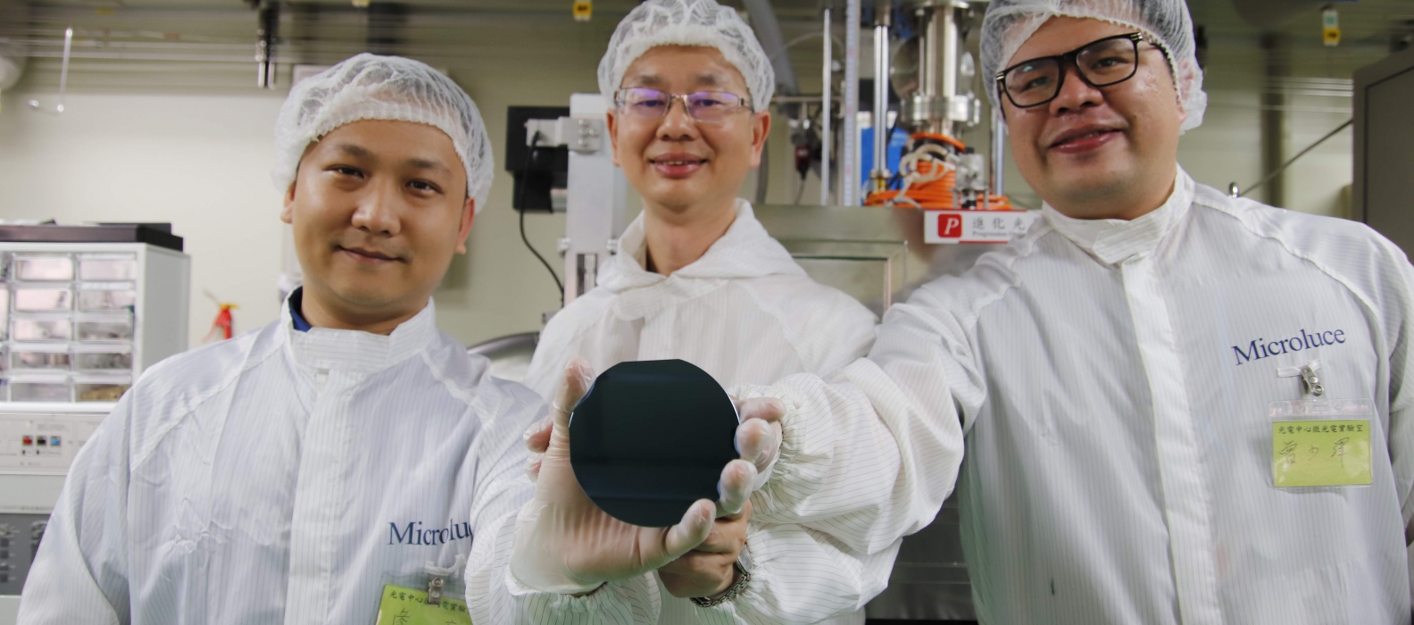
The Taiwan tech publication Digitimes is reporting how researchers at National Central University in Taiwan have developed a process that produces LED wafers that wouldn’t need mass transfer to make display panels.
I won’t get into the details because they’re VERY technical, and waaaay the hell over my pointy head. But it involves lowering the heat needed to make the wafers where LEDs are, for a lack of a better term, grown. The method entails use of nanometer material technology to make micro LED display panels instead of mass transfer process and incurs much less production cost than that for the latter.
I mention all this because of the description in the piece about the time and therefore cost involved, currently, to do microLED displays:
Mass transfer is a lengthy and expensive process, taking one hour to mass transfer 25,000 micro LED chips on correct positions in array on back planes, according to Microluce (a startup associated with the university). As a smartphone-used micro LED panel consists of about 11 million micro LED chips, mass transfer process will take as long as 18.3 days.
So if a 6″ smartphone screen would take 18 days, just imagine how long it would take to make a big-ass microLED video wall, like the Sony Clear LED. Either years, or many machines doing the same thing.
The research team, Digitimes reports, has also developed manufacturing equipment for the new method and has obtained patents in Taiwan and the US, Microluce indicated, adding it is cooperating with a Hong Kong-based driver IC design house in preparation for producing 1.8-inch micro LED display panels for use in smart wearables.
The sense I get from looking into miniLED and microLED is that while products are coming out now, like Sony’s and Samsung’s The Wall, we’re likely a couple of years out from broader commercialization, as manufacturing R&D is still working on the challenges.
The other issue with microLED is manufacturing yield – absolutely minimizing the numbers of dead or flawed pixels in production. On a large display, even at 99.999% success there would be potentially 1,000s of microLEDs that need repair or replacement.
Leave a comment